website logo
HomeShopDocsBlogForum
⌘K
Flipper Zero Documentation
Basics
🐬First start
Reboot
Control
Settings
SD card setup
Firmware update
Power
Sub-GHz
Reading signals
Reading RAW signals
Adding new remotes
Supported Sub-GHz vendors
Frequencies
125 kHz RFID
Reading
Emulation
Adding manually
Writing to an empty tag
Animal microchips
NFC
Reading NFC cards
Infrared
GPIO & modules
iButton
Bad USB
U2F (Universal 2nd Factor)
Applications
HID controllers
Flipper Mobile App
Reporting Mobile App bugs
qFlipper
Troubleshoot drivers on Windows
Development
Firmware
Hardware
Blueprints
Docs powered by archbee 
20min

Flipper Zero schematics

Document image

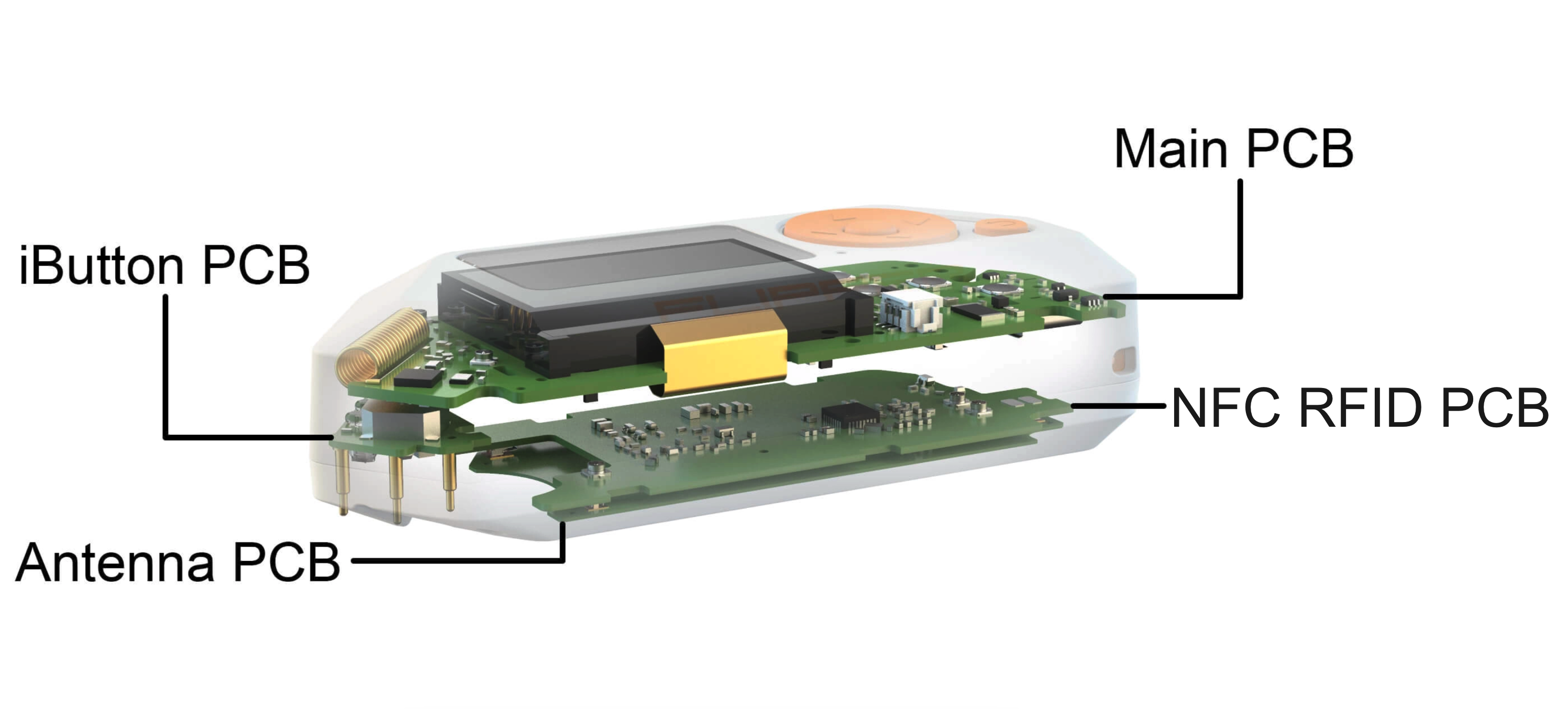
These are schematics of all Flipper Zero PCBs. They could be useful for hardware module development and low-level debugging. These schematics are for educational purposes only.

Main PCB

Document image

Main blocks overview

Every block is shown in detail as a separate document below.

Power

Power management system for all components.

Peripherals

MCU STM32WB55

LCD Display

Sub-1 GHz CC1101

Buttons

iButton PCB

Piezo speaker and IR are also placed on this PCB.

Document image

NFC RFID PCB

This PCB contains RFID 125 KHz and NFC modules.

Document image

NFC blocks overview

NFC

Power and vibro

RFID

Antenna PCB

Document image
Updated 15 Aug 2022
Did this page help you?
Yes
No
UP NEXT
ST-Link V3 Developer Board
Docs powered by archbee 
TABLE OF CONTENTS
Main PCB
Main blocks overview
Power
Peripherals
MCU STM32WB55
LCD Display
Sub-1 GHz CC1101
Buttons
iButton PCB
NFC RFID PCB
NFC blocks overview
NFC
Power and vibro
RFID
Antenna PCB

Community

Kickstarter Habr.com Discord Forum Blog

For developers

Documentation GitHub Design Guide

Partners

Neuron Hackerspace Design Heroes Slozhno.Media Lab401 Joom Hacker Warehouse

About

Contacts Compliance Company Careers Press kit Privacy Policy

Copyright © 2023 Flipper Devices Inc.